Finally I got time to continue the nixie clock. This week is the annual autumn break so hopefully I can make most parts of the clock ready. Writing program code is so time consuming that it is necessary to leave it for a later time. Yesterday I started to assemble the mainboard for the clock. It went mostly without any problems (I dropped my N900 phone which broke down and burned my fingers as usual), and I finished it tonight.
 Board in the right is the mainboard. It looks little bodgy, I didn’t have as much patience as before making a nixie controlboard from leftside of image. This time I didn’t floodsolder traces, but used striped single core wire.
  As you can see the mainboard is much more clearer and simpler. I did not fully flow schematics and layout plan. I moved some connector and traces, completely rearranged RTC’s battery and crystal and added leds for 5v and 170v indication. Later can be also used when debugging because it is software controlled(control signal for nixie swich mode psu).
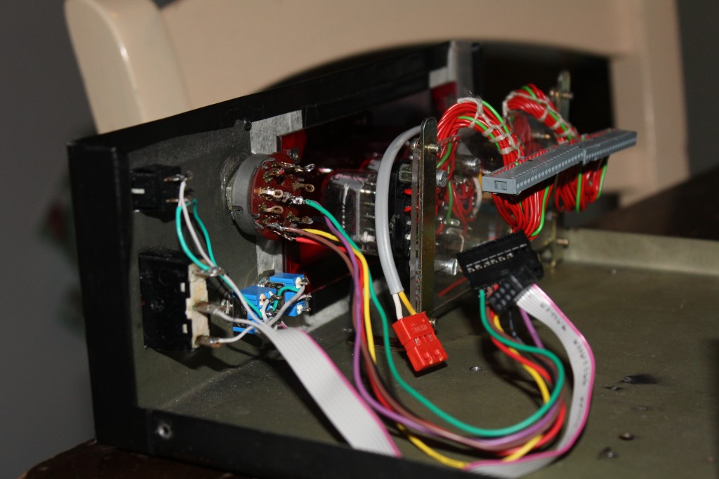
I also wired frontpanel switches to connectors. I’m not yet entirely sure about a rotary switch configuration, so I connected some extra contacts. I am also still thinking where to place mainboard. Therefore I left some excess length to the wires. Again, those bloody single core wires. But I’m out of normal proper wires, and in the other hand striping and crimping connectors to multicore wires are not too easy compared to single cores.
I have still much work to do. I need to make little board for nixie power supply with adjustment pot and connectors, and also make cables to connect different boards together. But thats for tomorrow, I have had too much burns and solder fumes for one day.
PS. Oh the N900, I left it on the table, and I had message or something and vibration alarm went on while it was charging. So vibration drove the phone on to edge of the table, and yar down the plank. Later I noticed that phone did not charge anymore and battery went dead. I opened phone on found out that micro USB connector were ripped from the PCB. I can’t rework so tiny pads under the connector, and parts from the traces is destroyed, so I might throw whole **** into the waste basket. Or maybe I can solder normal usb cable to test bads under the phone battery, which are connected internally to usb circuitry, could be worth of trying. I might still need to buy new phone, but I have absolutely no money to use and personally I hate symbian, iOS and windows phone, and I become anxious when using android because of dark and illogical menus and thousands useless programs(like talkin tom cat, wtf). </rant>
